Good! You decided to stay. Welcome back to the madness.
Our journey begins with a simple question—WHERE DO I EVEN START?!
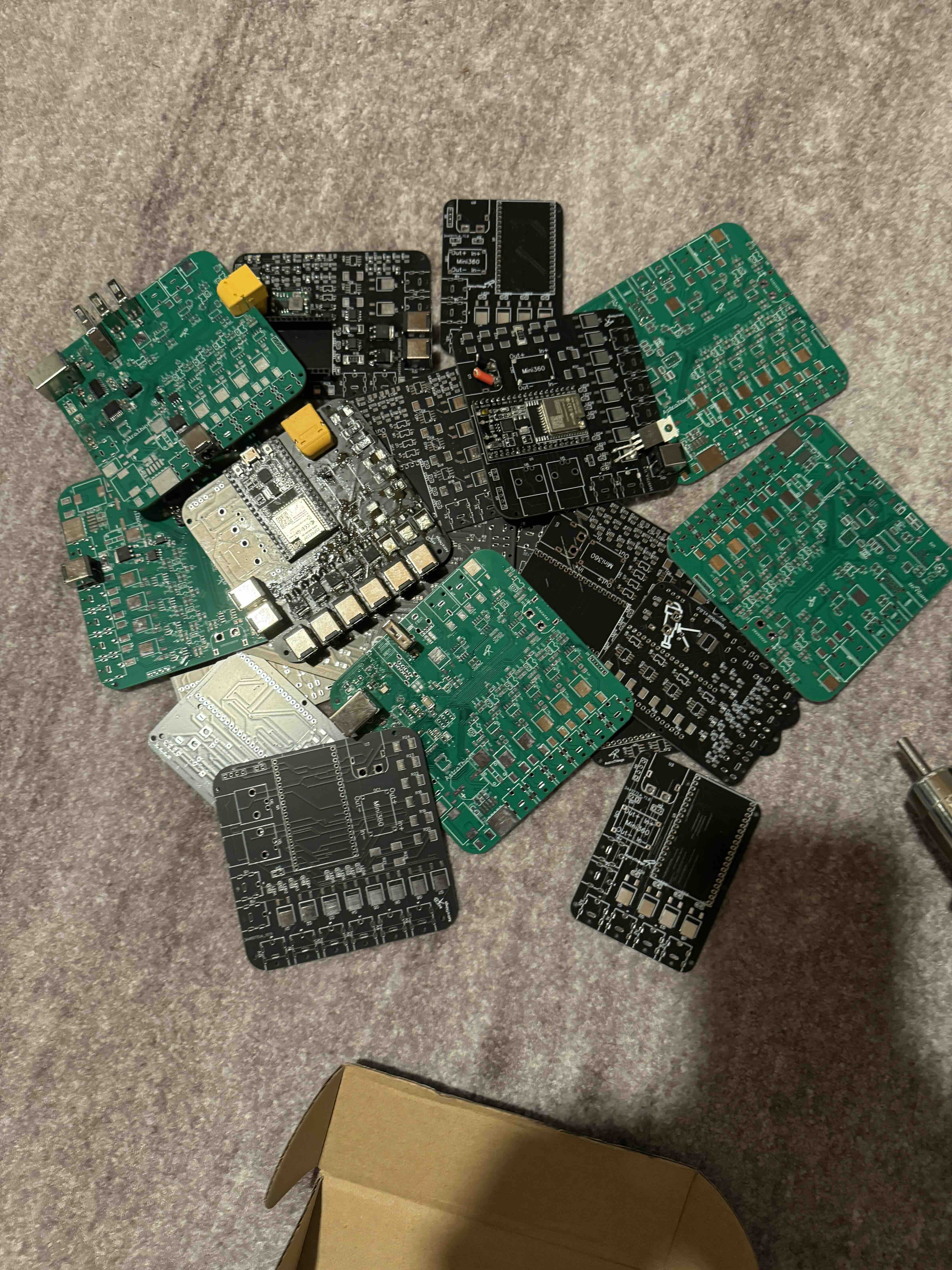 I’ve built projects before, but this was the first time I had to mess with electricity that was responsible for powering very expensive equipment. No pressure, right? But hey, baby steps. I got this. Okay, maybe by the 30th iteration… (RIP to my many failed attempts, forever resting in the graveyard of dead components.)
Honestly? Totally worth it.
That’s the beauty of being a maker. If you don’t know how to do something? Read. Ask. Experiment. Fail spectacularly. Repeat. Eventually, you’ll know enough to build whatever you want. Patience and persistence—remember that.
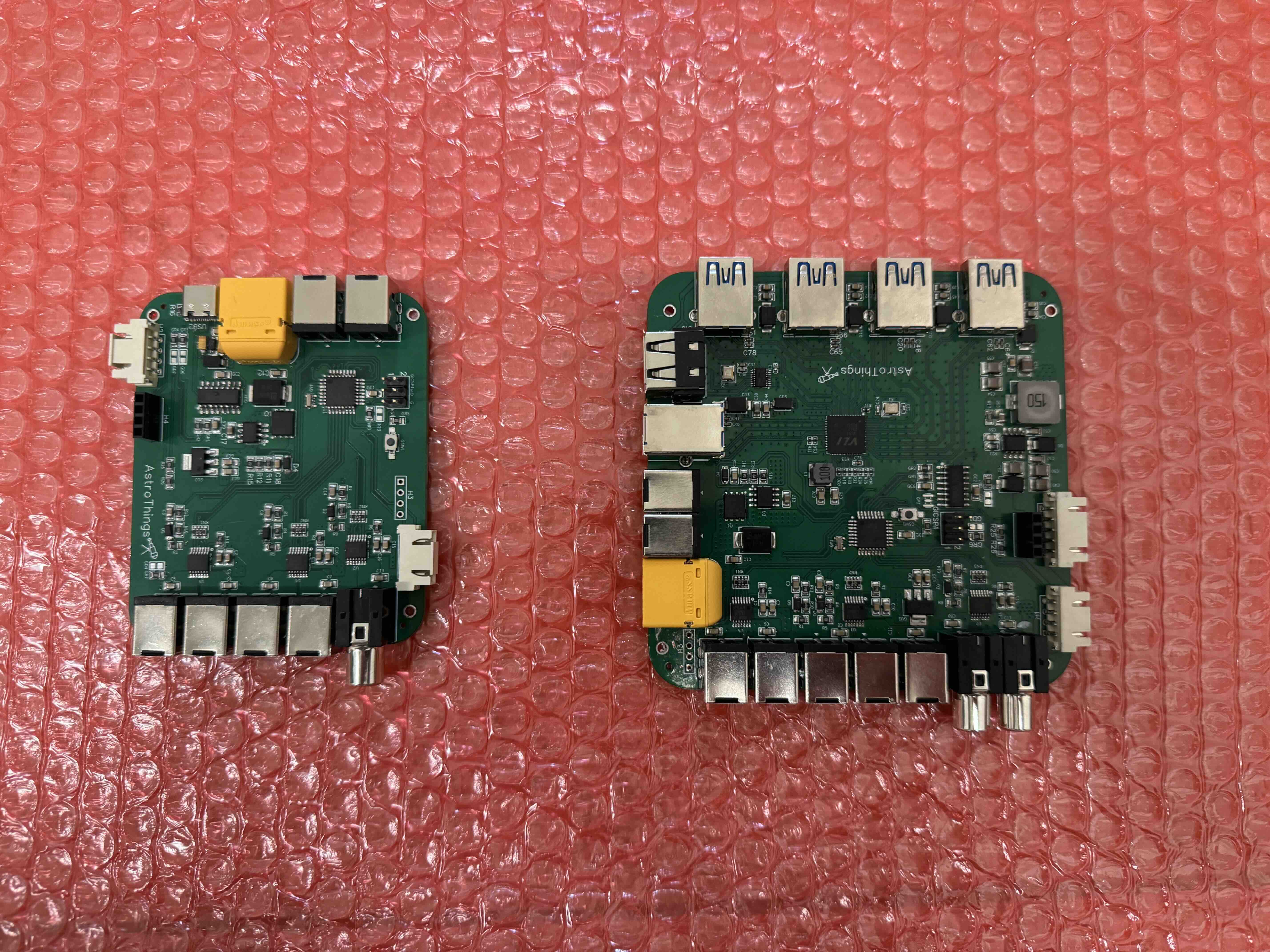
Version 1: The “Essential” Edition
I started with the Essential version (because at that point, there was no “Pro” yet). With each iteration, things got better:
- A big-ass MOSFET became a tiny I2C chip.
- A full ESP32 board shrank into an embedded ATMEGA microcontroller.
- A weak, sketchy step-down module transformed into a robust, safe, PCB-embedded one.
- Bulky SMT components got downsized to tiny 0402 parts.
- A 2-layer PCB evolved into a 4-layer PCB.
- And an old-school USB mini got replaced with USB-C (because it’s 2025, people!).
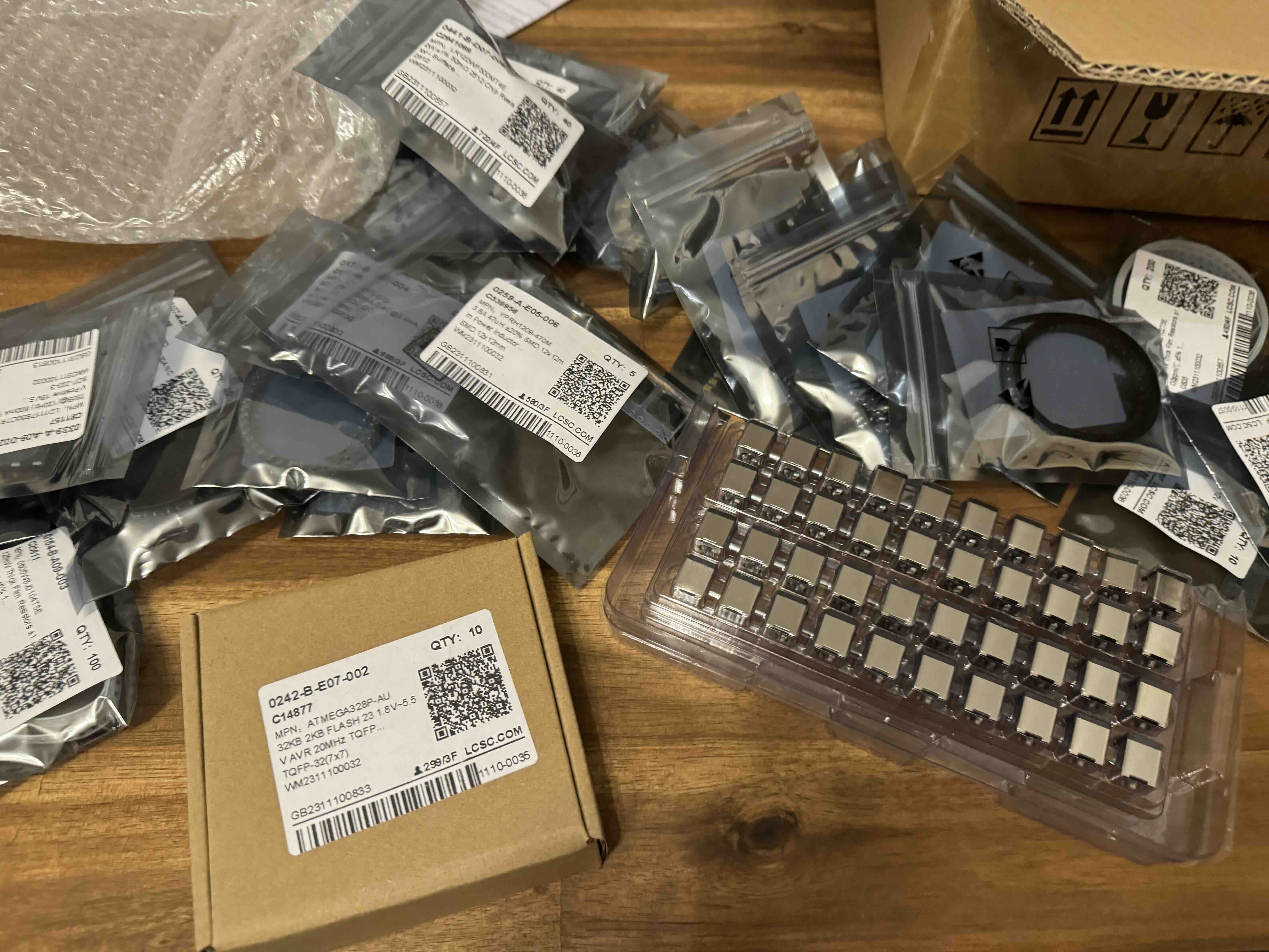
Selecting the right components was its own adventure. Everything had to fit just right — voltage ratings, temperature tolerances, size, features. And yeah… sometimes (most of the time), I had to start over. But in the end, every single part had to work in perfect harmony to get the best price-to-performance ratio.
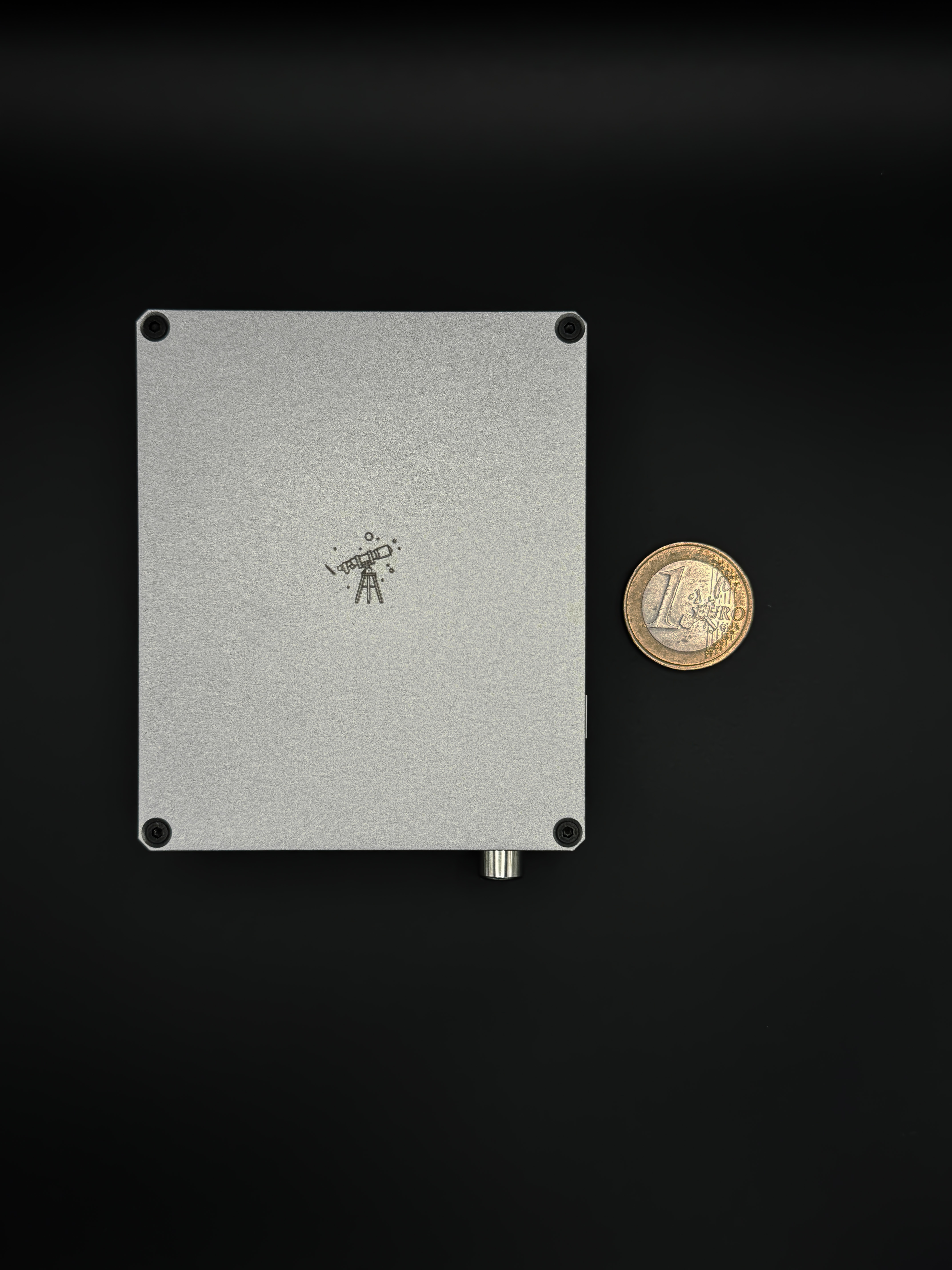
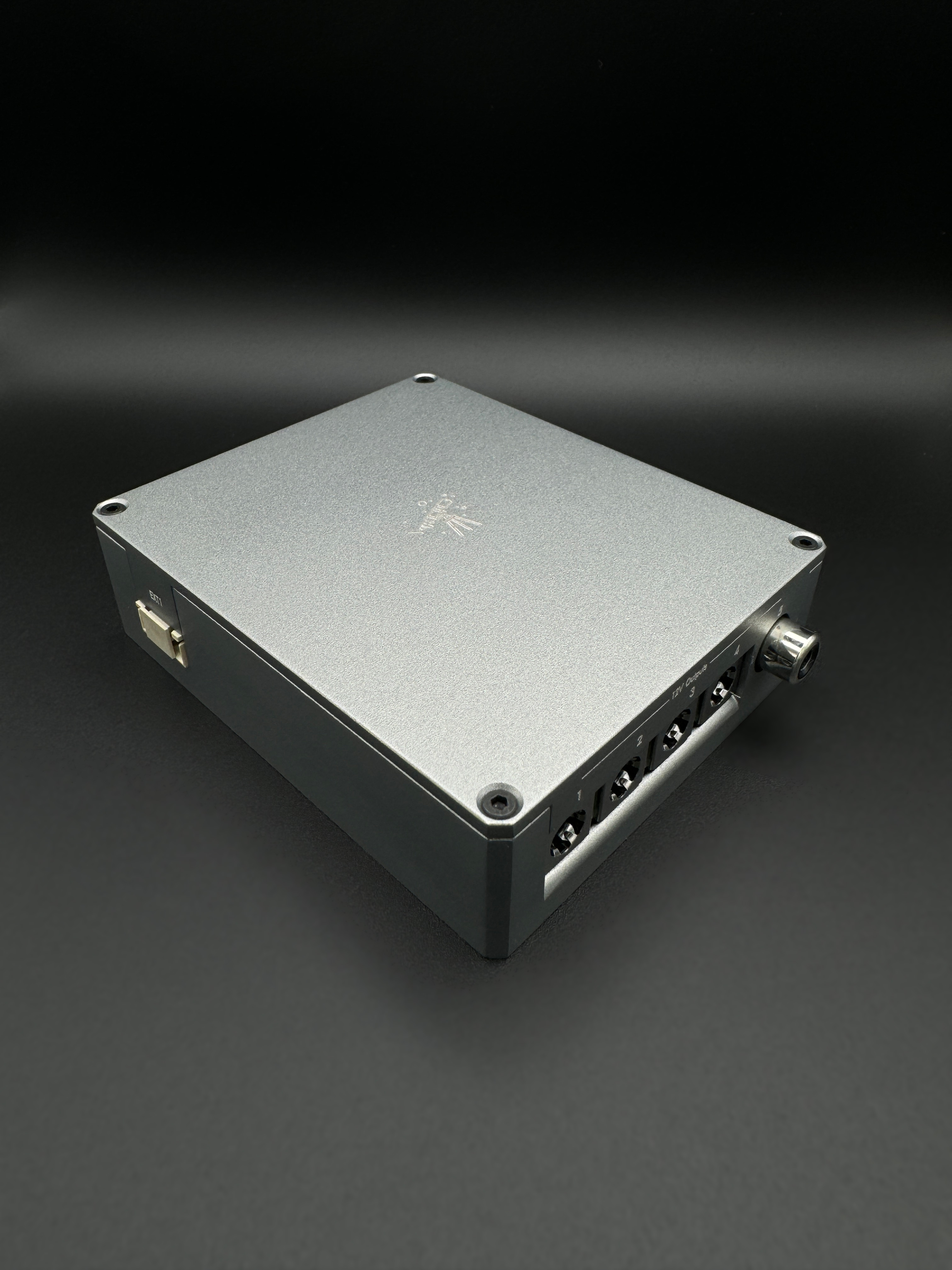
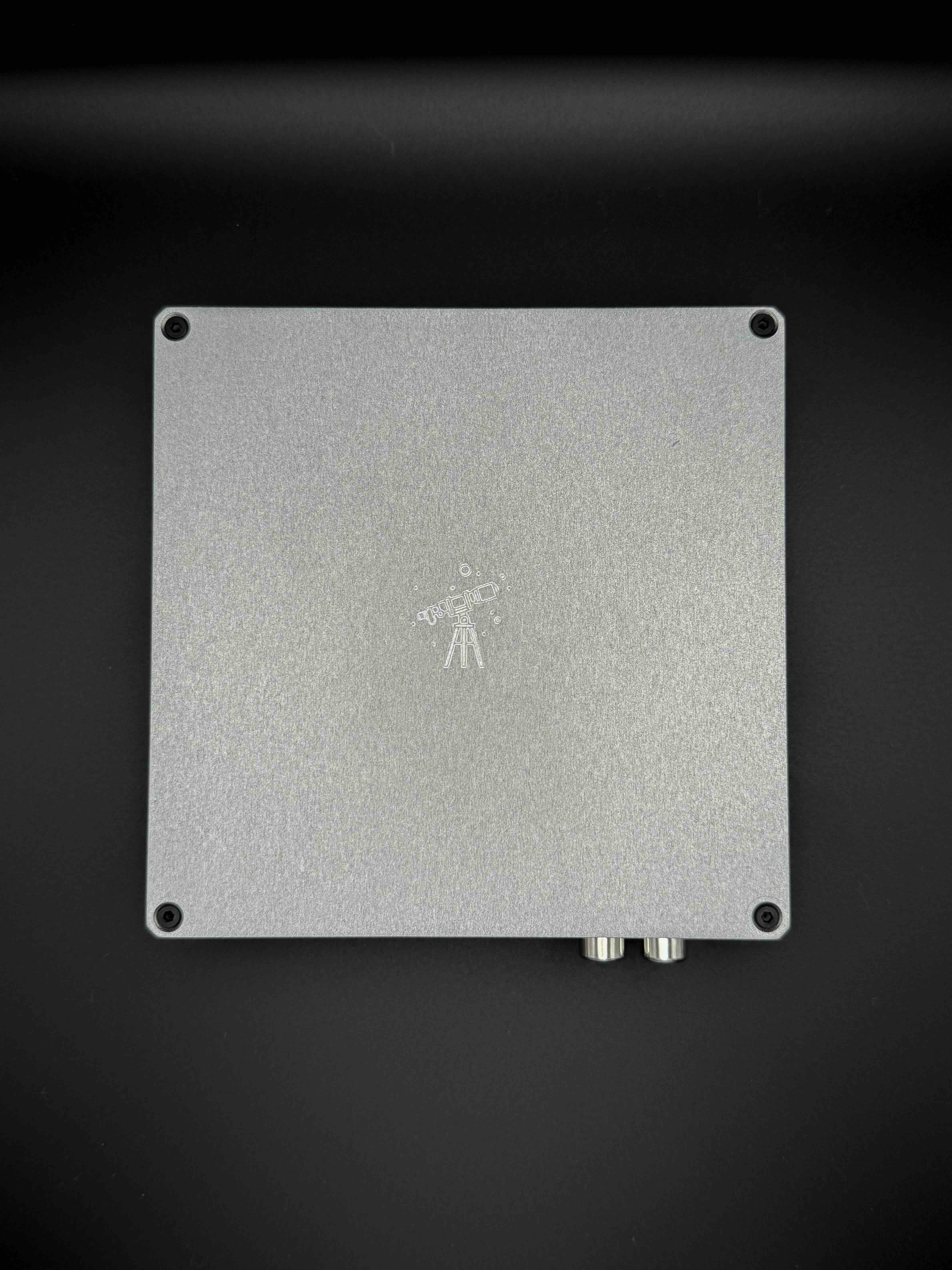
The result? A tiny, mighty Essential PCB measuring just 83mm × 68mm — all while keeping costs rock-bottom:
- Assuming you solder everything yourself, and order the CNC enclosure - about 120 Euros, yes, you read it right.
- If you want that all the soldering is done for you, (and you also know where to get the components) it will cost about 150 Euros.
- Want to lower the cost even more - you can 3D print the box and solder everything yourself and your cost can be slashed to 40 Euros (!!!).
Can you guess the margins on similar products in the market? Yeah… I did too.
Leveling Up: The “Pro” Edition
Now, the Pro version came with its own set of nightmares—I mean, challenges:
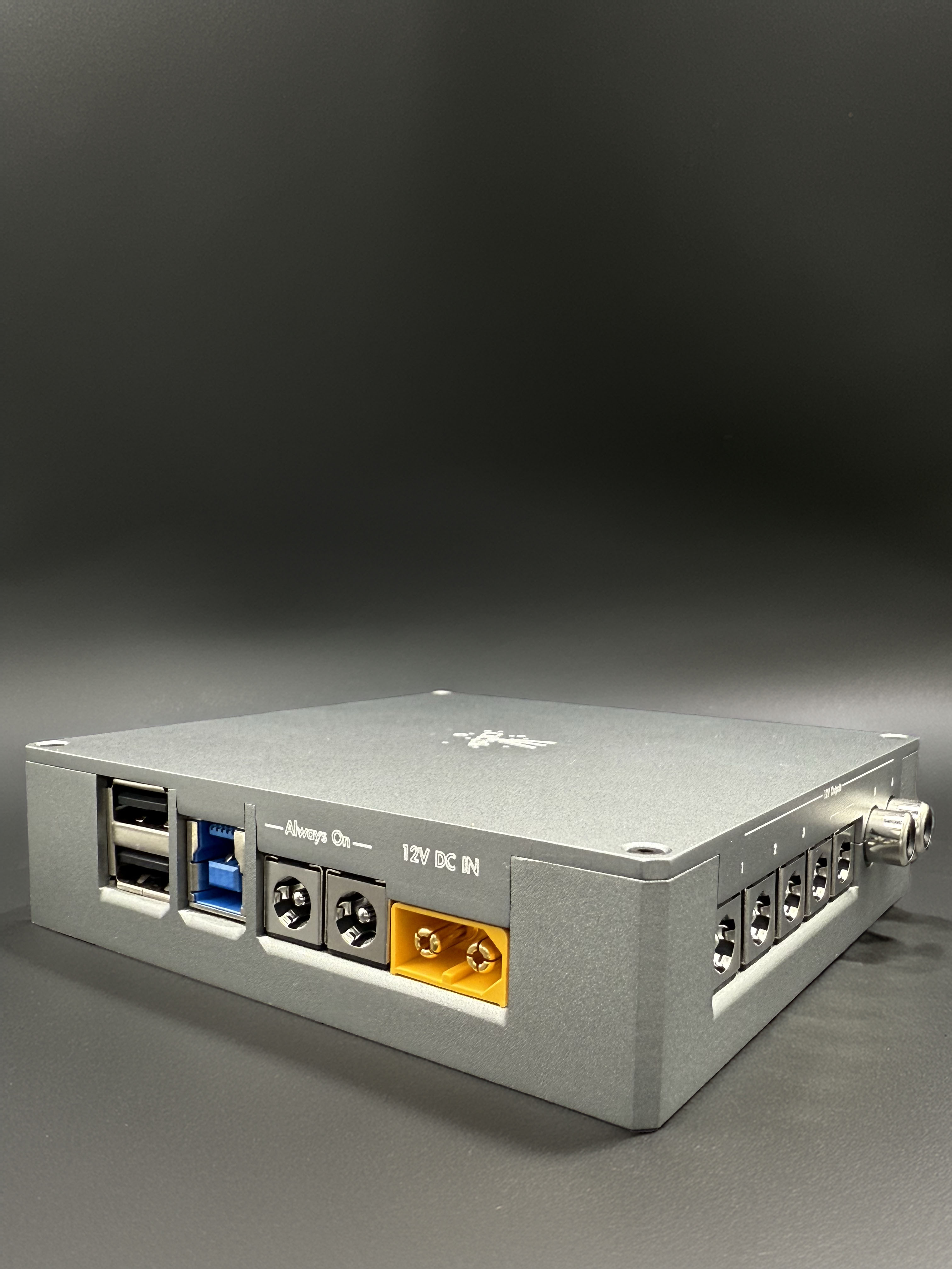
- USB 3.0 Hub Design – Turns out, designing a USB3 hub isn’t as simple as USB2. There are a lot of variables to consider: signal integrity, interference, grounding, data speeds… basically, a whole bunch of things I didn’t even know existed until I had to fix them.
- Size Constraints – To keep manufacturing costs down, the PCB had to stay under 100mm × 100mm. Go beyond that, and you get hit with a premium fee. And that wasn’t happening. Not in my house.
USB 3.0: The Pain, The Struggle, The Victory
If you’ve ever tried designing a USB3 hub, you’ll know that finding useful resources is like hunting for unicorns. There’s barely any documentation, tons of engineering rules, and a lot of trial and error involved.
After days of scouring the internet, I finally hit gold—a guide from Texas Instruments. This thing had all the rules I needed to follow, and let me tell you… some of them were weird.
Of course, my first few USB3 hubs didn’t even work. Then they worked… but constantly lost connection. Then they were slower than a floppy disk. Then they went back to not working at all. Fun times.
To make it even more “fun,” I decided to hand-solder everything to save costs. Picture soldering tiny 0402 components and a USB chip with a QFN-76 package (which I’m convinced was designed by the devil himself). Yeah… let’s just say, I was this close to giving up.
But persistence pays off! Not only did I finally nail it, but I even threw in an extra USB2.0 hub just because I could—all while staying under 100mm × 100mm. Take that, premium PCB fees!
I know, I know. Some haters will say, “bUt tHEre aRe smALLer pROdUcTS oUt tHEre”. To them, I say: go read the reviews. See how well those USB3 hubs perform on cold nights. Check their price-to-performance ratio. Then come back and tell me who’s winning. 😉
Next Steps: The Enclosure, Drivers & Software
Now that I had a fully functional PCB, it was time to tackle the next phase—building the enclosure, writing the drivers, and developing the software. But before we dive into that, I’ll be sharing more about the PCB details and components in the next post.
For the curious minds out there, you’ll also find all the files to build your own PowerBox. Stay tuned!
Send me an email or use the contact form
Want to buy me beer 🍻? Use this link
See you next time!
~The Bright Knight